If you're looking for a rough estimate of how fast a given gfx card is, look at the texel fill rate and the triangle setup capabilities.
* THIS IS A WORK IN PROGRESS! *
by Peter Bjørn Perlsø
created 1st of September 1999 (first draft April 1999)
updated 30th of September 2006, and 30th of August 2009
Additions and corrections are welcome. I will update this article as time allows for it.
The purpose of this article is to give an authoritative representation of the progress in the field of computerized graphics acceleration, primarily 3D.
Related and useful articles:
+ How much bandwidth does the various buses provide?
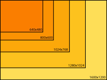
Fill rate: The (pixel) fill rate is quite simply, how many pixels on the computer display, your graphics hardware can alter (fill with new data) per second. But how much is a mega pixel really in practical terms? Take a look at the graphic below:
If you're looking for a rough estimate of how fast a given gfx card is, look at the texel fill rate and the triangle setup capabilities.
| resolution | pixels | proportion | |
| 320 x 200 | 64 K | 16:10 | |
| 320 x 240 | 76.8 K | 4:3 | |
| 512 x 384 | 196.6 K | 4:3 | |
| 640 x 400 | 256 K | 16:10 | 4* 320 x 200 |
| 640 x 480 (VGA) | 307.2 K | 4:3 | 4* 320 x 240 |
| 640 x 512 | 327.68 K | 5:4 | |
| 800 x 600 (SVGA) | 480 K | 4:3 | |
| 832 x 624 | 519.2 K | 4:3 | |
| 1024 x 768 (XGA) | 786.4 K | 4:3 | 4* 512 x 384 |
| 1152 x 768 | 884.8 K | 3:2 | |
| 1280 x 1024 | 1.31 M | 5:4 | 4* 640 x 512 |
| 1440 x 900 | 1.26 M | 16:10 | |
| 1600 x 1200 | 1.92 M | 4:3 | 4* 800 x 600 |
| 1680 x 1050 | 1.76 M | 16:10 | |
| 1920 x 1200 | 2.3 M | 16:10 | |
| 2560 x 1600 | 4.1 M | 16:10 | |
As you can see from the above table, the pixel counts climb into the millions pretty quickly as you increase your display resolution. To determine how high a fill rate you need, you can use this formula:
horizontal resolution * vertical resolution * desired frame rate = target fill rate
So, for example, to play your favorite 3D game in 1600*1200 pixels with 60 frames per second (fps), you'd need a graphics chip that can pump out 1600*1200*60 = 115,2 million pixels per second. By modern graphics hardware, this is easily achieved.
Stencil Buffer: Pixel-based buffer used by graphics accelerators to store effect information for individual pixels. A stencil buffer 8 bit wide would allow for 256 (2^8) effect layers "on top" of each pixel. Usually employed in conjunction with a z buffer for effects such as fogging, shadowing etc.
Z Buffer: Pixel-based depth buffer used to determine the visibility of pixels in a rendered scene. The buffer provides a way for the renderer to determine whether a rendered pixel should be sent to the frame buffer, by comparing z (depth) values for each pixel in the rendered
polygons. The smaller the z value for a pixel, the closer it is to the observer. If a rendered pixel has a lower z value than an already rendered pixel, its color information overwrites that if the "old" pixel.
Key to charts:
MP = Mega Pixels, MT = Mega Texels, GP = Giga Pixels , GT = Giga Texels
| Card,chip | fill rate | pixel pipes, texel units per pipe, vertex pipes | triangles | core clock | core transistor count | memory size and type | mem clock | RAMDAC clock | interface | comments | ||
| Voodoo Graphics | 45 MP | ?,1,- | 1 M | .50µ | 4-6?M EDO | 135? | PCI | 180$? 1997, 640x480 3D only | ||||
| Voodoo Rush | 1 M | .50µ | 4-6-8M EDO, 128b | PCI | both 2D and 3D gfx, many driver problems | |||||||
| Voodoo 2 (1000) | 90 MP | ?,2,? | 3 M | 90 | 8-12M EDO | PCI | 1H 1998 , up to 800x600, 3D only, SPMT, SPTF, FTS, SLI (1024x768), rendering 32bpp internally, 16 bpp externally (output to frame buffer), textures up to 256^2 pixels, multitexturing | |||||
| Voodoo Banshee | 100-125 MP | 4 M | 100, 125 | .35µ, .25µ | 16M | 100 | 250 | PCI, 1x AGP | both 2D and 3D, only one texture unit | |||
| Voodoo 3 2000 | 143 MP | ?,2,? | 6 M | 143 | 8.2M | 16M SDRAM (8x faster block writes and Z-clears) | 300 | PCI, 2x AGP | 128-bit accelerator, up to 1920x1440 (3D), 2048x1536 (2D), RAM bandwidth 2.29 GBps, but still no 32bpp rendering or 32b texture support. Readded the second texturing unit that was originally removed from the Banshee, 16b Z-buffer | |||
| Voodoo 3 3000 | 167 MP | ?,2,? | 7 M | 166 | 16M SD | 350 | " | RAM bandwidth 2.66 GBps | ||||
| Voodoo 3 3500 TV | 366 MT | ? | 8 M | 183 | 16M SD | 350 | 2x AGP | RAM bandwidth 2.92 GBps | ||||
| Voodoo 4 4500 | 333-366 MP | 1*2,1,? | 166 | 14 M @ .25 µ | 32M SD | PCI, 4x AGP | late 1999, V4's and V5's based on VSA-100 chips (Voodoo Scalable Architecture), 2048^2 pixel texture support, and FINALLY 32 bpp output & textures (RGBA), 24b Z&W buffers, 180$ | |||||
| Voodoo 5 5000 | 667-733 MP | 2*2,1,? | 166 | 32M SD | " | 2 VSA chips (SLI!) - 2 pix/clock, 1 tex/pix - all V5 cards require their own PSU! 230$ | ||||||
| Voodoo 5 5500 | " | 2*2,1,? | 166 | 64M SD | 166 | ? | 4x AGP | 300$ | ||||
| Voodoo 5 6000 | 1.33 - 1.47 GP | 4*2,1,? | 166 | 128M SD | " | 4 VSA chips - broke 1 gigapixel barrier, 600$ | ||||||
| Voodoo 6 | rumored, but never materialized | |||||||||||
SPMT = Single Pass MultiTexturing, SPTF = Single Pass Trilinear Filtering, FTS = Full Triangle Setup (offloads CPU)
SLI = Scan Line Interleaving, allows you to combine two gfx cards into one logical card.
VSA-100: 8-bit stencil rendering, and advanced texture and color combine capabilities, DVD hardware assist. DXTC. T-buffer - not on V4 cards, only V5 (full screen antialiasing (FSAA), motion blur, programmable depth-of-field, oft shadows and reflections etc.)
| Card,chip | fill rate | pixel pipes, texel units per pipe, vertex pipes | triangles | core clock | core transistor count | memory size and type | mem clock | RAMDAC clock | interface | comments | ||
| RIVA 128 (NV3), 128ZX (NV3.5) | 100+ MP | 1,1 | 5 M | 100 | 4 M SGRAM (ZX: 8 M) | 100 | PCI | summer 1997, 16b Z-buffer | ||||
| RIVA TNT (NV4) | 180+ MP | 2,1 | 6 M | 90+ | 7 M @ .35µ | 4-8-16 M SDR, 128b | 110+ | 250 | PCI, 2x AGP | 150$ (8M) 200$ (16M) summer 1998, TNT = TwiN Texel, 128b engine, 32bpp color, 24b Z buffer, 8b stencil buffer | ||
| TNT 2 (NV5) | 250+ MP | 2,1 | 9 M | 125+ | 10 M @ .25µ | 32 M SDR | 150+ | 300 | 2x AGP | Spring 1999 , up to 1600x1200 | ||
| TNT 2 Ultra | 300+ MP | 2,1 | 9 M | 150+ | SDR | 183+ | 2x AGP | |||||
| TNT 2 Pro (NV6) | 143 | 166 | ||||||||||
| Geforce 256 (NV10) | 480 MP | 4,1 | 120 | 23 M @ .25µ | SDR/DDR | 166 | 4x AGP | Summer 1999, T&L | ||||
| Geforce 2 | ||||||||||||
| Geforce 2 GTS (NV15) | 800+ MP | 4,2,? | 25 M | 200+ | .18µ | 32 M DDR | 167+ | 350$, Summer 2000, GTS = Geometry, Transformation, Shading - bump mapping, cube environment mapping etc, Dual Texel Pipeline, replaced Geforce 256 | ||||
| Geforce 2 Ti (NV15A) | 250 | 200 | ||||||||||
| Geforce 2 MX (NV11) | 350 MP | 2,2,? | 20 M | 175 | .18µ | 32M DDR SGRAM | 166 | 350 | PCI, 4x AGP | 150$, 2 dual-texturing pipelines (700 MT) , replaced TNT 2 | ||
| Geforce 2 MX 100 | ||||||||||||
| Geforce 2 MX 200 | 350 MP | 2,2,? | 64 M DDR | |||||||||
| Geforce 2 MX 400 | 400 MP | 2,2,? | 200 | 183 | 350 | |||||||
| Geforce 3 Ti200 (NV20) | 175 | 57 M | up to 128 M DDR | 200 | 350 | 4x AGP | ||||||
| Geforce 3 Ti | " | 230 | 350 | 4x AGP | ||||||||
| Geforce 3 Ti500 | 240 | " | 250 | 350 | 4x AGP | |||||||
| Geforce 4 Ti 4200 (NV 25?) | 113 M | 250 | 63 M @ .15µ | up to 128 M DDR | 222 | 4x AGP | 200$ Spring 2002 | |||||
| Geforce 4 Ti 4400 | 125 M | 275 | " | 275 | 4x AGP | 300$ Spring 2002 | ||||||
| Geforce 4 Ti 4600 | 136 M | 300 | " | 325 | 4x AGP | 400$ Spring 2002 | ||||||
| Geforce 4 Ti 4800 | " | 8x AGP | ||||||||||
| Geforce 4 MX 420 (NV17) | 1 GT | 2,2,.5 | 31 M | 250 | .15µ | up to 64 M SDR 128b | 166 | 2x 350 | 4x AGP | |||
| Geforce 4 MX 440 (NV 18?) | 540 MP | 2,2,.5 | 34 M | 275 | up to 64 M DDR 128b | 200 | 2x 350 | 4,8x AGP | ||||
| Geforce 4 MX 460 | 1.2 GT | 2,2,.5 | 38 M | 300 | " | 275 | 4x AGP | |||||
| Geforce 5200 FX (NV 34) | 1 GT | 2,2,? | 250 | 45 M @ .15µ | DDR | 200 | ||||||
| Geforce FX 5200 Ultra (NV 34 Ultra) | 2,2,1 | 325 | DDR | 325 | 2x 350 (400?) | 8x AGP | used in Apple iMacs , replaces MX 440 | |||||
| Geforce FX 5500 | 1.1 GT | 128b | 2x 350 | |||||||||
| Geforce FX 5600 (NV 31) | 2,2,? | 300 | .13µ | DDR | 250 | 2x 400 | ||||||
| Geforce FX 5600 Ultra (NV 31 Ultra) | 1.6 GP ? | 2,2,? | 350 | 75 M @ .13µ | DDR | 350 | 2x 400 | replaces Ti4200 | ||||
| Geforce FX 5700 (NV 36) | DDR-II | 475 | replaces FX 5600 | |||||||||
| Geforce FX 5800 (NV 30) | 1.6 GP ? | 4,2,? | 200 M ? | 400 | 125 M @ .13µ | 128-256 M DDR-II | 400? 450? | 2x 400 | 8x AGP | summer?/fall 2002, 512b core | ||
| Geforce 5800 Ultra (NV30 Ultra) | 2 GP ? | 4,2,? | 500 | 125 M @ .13µ | DDR-II | 500 | 2x 400 | replaces Ti4800 | ||||
| Geforce 5900 Ultra (NV 35?) | 1.8 GP ? | 4,2,? | 450 ? 500 ? | .13µ | 128 - 256 M DDR -II 256b ? | 425 ? 500 ? 600 ? | 2x 400 | 8X AGP | spring 2003 ? | |||
| Geforce FX 5950 (NV 38) | 475 | DDR-II | 475 | replaces FX 5900 | ||||||||
| Geforce 6200 | ||||||||||||
| Geforce 6600 GT + Ultra | ||||||||||||
| 6800 GT + Ultra DDL (NV 40) | 5.6 GP + 6.4 GP | 16,1,6 | 350 + 400 | 500 + 550 | dual DVI | |||||||
| Geforce 6800 Ultra Extreme (NV 45) | 16,1,6 | 450 | 300 | 2x 400 | the marketing department should be sacked on the spot for coming up with such a name | |||||||
| Geforce 7800 GTX (G70) | 24,1,8 | 430 | 256, 512 MB | 600 | 24 pixel shaders | |||||||
| Geforce 7800 GT (G71) | 20,1,8 | 400 | 500 |
| Card,chip | fill rate | pixel pipes, texel units per pipe, vertex pipes | triangles | core clock | core transistor count | memory size and type | mem clock | RAMDAC clock | interface | comments | ||
| Geforce4 410 Go | ||||||||||||
| Geforce4 420 Go | 800 MT | ? | 200 | |||||||||
| Geforce4 440 Go | 880 MT | ? | 220 | |||||||||
| Card,chip | fill rate | pixel pipes, texel units per pipe, vertex pipes | triangles | core clock | core transistor count | memory size and type | mem clock | RAMDAC clock | interface | comments3D | ||
| RAGE | 20 MT ? | 40 ? | 2 M EDO | 135 | PCI | first ATI 3D offering | ||||||
| RAGE II/II+ | 25 MT ? | 50 ? | 2,4,6,8 M EDO & SDRAM | 135 | PCI | MIP map, Gouraud shading, alpha blending and fog effects | ||||||
| RAGE IIc | 25 MT ? | 50 ? | 4,8 (AGP only) M SD/SGRAM | 200 | PCI, 2xAGP | 64b core , AGP support | ||||||
| RAGE Pro | 75 MP | 1?,1,- | 1.2 M | 75 | .25µ | 2-4-6-8-16 M SGRAM | 100 | 230 | PCI, 2x AGP | Spring 1997, sported hardware multitexturing with one pipeline | ||
| RAGE 128 | 200 MP | 2?,1,- | 4 M | 75,90,100 | 32 M | 2x AGP | Autumn 1998, numerous driver problems | |||||
| RAGE 128 Pro | 250-286 MP, | 2,1,- | 8 M | 125,143 | 16,32 M, 128b | 143 | 300 | 4x AGP | Feb. 99 ? | |||
| RADEON (7000) | 1.6 GT | 64 M SDR, 32 M DDR 256b | 166? | 300 | 4x AGP | many driver problems | ||||||
| Radeon 7500 (RV200) | 580MP | 2,3,? | 270, 290 | .15µ | 64 M DDR, 128b | 230 | 2 x 350 MHz | PCI, 2,4x AGP | sept 2001 , 199$, | |||
| Radeon 8500 (R200) | 1.1GP | 4,2,2 | 65 M | 250 | 60 M @ .15µ | 64, 128 M DDR, 128b | 275 | 4x AGP | sept 2001, 399$ | |||
| Radeon 9000 (RV250) | 1GP | 4,1,1 | 75 M | 250 | 32,64,128 M dual channel DDR, 128b | 200 | 2 x 400 MHz | |||||
| Radeon 9000 Pro | 1.1GP | 4,1,1 | 75 M | 270 | 40 M | 64,128 M dual channel DDR, 128b | 275 | 129$, summer 2002 | ||||
| Radeon 9500 (R?) | 1.1GP | 4,1,4 | 275 M | 275 | .15µ | 64, 128 M DDR, 128b | 270 | |||||
| Radeon 9500 Pro | 2.2GP | 8,1,4 | 275 M | 275 | .15µ | 128 M DDR, 128b | 270 | |||||
| 9550 | 250 | 8x AGP | ||||||||||
| Radeon 9700 (R300) | 2.5GP | 8,1,4 | 325 M | 300 | 110 M | up to 256 M DDR, 256b | 8x AGP | |||||
| Radeon 9700 Pro | 8,1,4 | 325 | DDR, 256b | 8x AGP | ||||||||
| Radeon 9200 | 4,1,? | 250 | .15µ | 64, 128 M DDR, 128b | 200 | 2 x 400 MHz | 8x AGP | 80$, Spring 2003 | ||||
| Radeon 9200 Pro | 4,1,? | 275 | .15µ | 128 M DDR, 128b | 275 | 2 x 400 MHz | 8x AGP | 130$, Spring 2003 | ||||
| 9200 SE | 8x AGP | |||||||||||
| 9250 | 240 | 128 M DDR, 128b | 200 | 8x AGP | ||||||||
| Radeon 9600 | 1.3GP | 4,1,2 | 175 M | 325 (350?) | .13µ | 64, 128 M DDR 128b | 200 (275?) | 8x AGP | 150$, Spring 2003 | |||
| Radeon 9600 Pro (RV350) | 1.6GP | 4,1,2 | 175 M | 400 | .13µ | 128 M DDR, 128b | 300 | 8x AGP | 200$, Spring 2003 | |||
| Radeon 9600 XT (RV360) | 2GP | 4,1,2 | 500 | 128 M DDR, 128b | 300 | 400 | 8x AGP | Autumn 2003, tweaked R9600 core | ||||
| Radeon 9800 (R350) | 8,1,4 | 325 | 128 M DDR, 256b | 325 | 8x AGP | Spring 2003 | ||||||
| Radeon 9800 Pro (R350) | 3 GP | 8,1,4 | 380 | 115 M @ .15µ | 128,256M DDR, 256b | 350 | 8x AGP | 400$, Spring 2003 | ||||
| Radeon 9800 XT | 3.3 GP | 8,1,4 | 412 | 365 | 8x AGP | |||||||
| Radeon X300 | 400 | 200 | PCIe x16 | late 2004 | ||||||||
| X300 SE | 325 | |||||||||||
| Radeon X600 | PCIe x16 | |||||||||||
| Radeon X800 XT | 7.6 GP | 16,1,6 | 475 | 500 | PCIe x16 | late 2004, 500$ | ||||||
| Radeon X850 XT | PCIe x16 | |||||||||||
| X1600 | ||||||||||||
| X1800 (R520) XT | 512 MB RAM | November 2005, takes over where X850 let go. 16 pixel shaders | ||||||||||
| X1900 (R580) | followup to R520 , January 2006. 48 pixel shaders , 60 million more transistors than X1800, up to 175 Watt power dissipation. | |||||||||||
| Card,chip | fill rate | pixel pipes, texel units per pipe, vertex pipes | triangles | core clock | core transistor count | memory size and type | mem clock | RAMDAC clock | interface | comments | ||
| RAGE Mobility 128 | 210 MP | 8 M | 2x AGP | 32b Z-buffer | ||||||||
| Mobility Radeon | 15 M | 166 | 8-64 M, 32-64B | 166 | 4x AGP | |||||||
| Mobility 7500 | 40 M | 275 | 16-64 M, 64-128b | 175 | ||||||||
| Mobility 9000 | 1GP | 4,1,? | 250 | 32 M 64b, 64 M 128b DDR | 230 | |||||||
| Mobility 9200 | 250 | DDR, 128b | 225 | |||||||||
| Mobility 9600 (M10) | 1.2GP | 4,1,2 | 350 | DDR, 128b | 250 | 8x AGP | Spring 2003 | |||||
| Mobility 9700 (M11) | 1.8GP | 4,1,2 | 450 | DDR, 128b | 260 | 8x AGP | ||||||
| Mobility 9800 (M18) | 2.8GP | 8,1,4 | 350 | 300 | 8x AGP | |||||||
| Mobility X300 (M22) | 1.4 GT | 4,?,2 | 300 | PCIe x16 | ||||||||
| Mobility X800 (M28) | 4.8 GT | 12,?,6 | 400 | PCIe x16 | ||||||||
| Card,chip | fill rate | pixel pipes, texel units per pipe, vertex pipes | triangles | core clock | core transistor count | memory size and type | mem clock | RAMDAC clock | interface | comments | ||
| Millennium | ||||||||||||
| Millennium II | ||||||||||||
| Millenium G200 | 100 MP | 1.55 M | 8-16 M SGRAM | 250 | 2x AGP | 32 bbp rendering, 32b Z-buffer, Alpha-Blending, Bi-linear Filtering, Tri-linear MIP-Mapping, Fogging, Anti-Aliasing, Specular Highlighting |
||||||
| G400 | 120 | 300 | ||||||||||
| G400 MAX | 333 MT | 2,? | 150-166 | .25µ | 32M SGRAM | 200 | 360 | 4x AGP | ||||
| G450 | ||||||||||||
| G500 | ||||||||||||
| G550 | ||||||||||||
| G800 | ||||||||||||
| G1000 | ||||||||||||
| Card,chip | fill rate | pixel pipes, texel units per pipe, vertex pipes | triangles | core clock | core transistor count | memory size and type | mem clock | RAMDAC clock | interface | comments | ||
| S3 | ||||||||||||
| Virge GX | ||||||||||||
| Savage 4 | ||||||||||||
| Savage 4 Pro | BEING | WORKED | ON | |||||||||
| Permedia | ||||||||||||
| PowerVR | ||||||||||||
NOTES:
A texture unit is the same (performance wise) as a texel pipeline. You calculate the texel fill rate by multiplying the pixel fill rate by the number of texel/texturing units (TMU's).
Memory bandwidth is calculated by multiplying the memory bus width with the memory clock speed. Keep in mind that this will give you the peak speed (theoretical maximum). Fill rate is calculated by multiplying core clock by the number of pixel and texel pipelines in the chip.
- Rage Pro Turbo is really just a Rage Pro with a nice name. Turbo name was due to a software update that needed extra publicity from ATI, i think.
- RAGE 128 supports textures up to 2048^2 pixels.
- Rage 128 Ultra was a version of the 128 Pro with extra RAM (16 M in all) at a cheap price. Summer 2000?
- Radeon 8500 featured TRUFORM, SMARTSHADER. RADEON 8500LE was later renamed
9100.
Misc.
gfx segments, 2002:
100 $ - mainstream, 200 $ - high end, 300 $ - ultra high end
will be added at a later time :
definitions and explanations of:
texel fill rate, GPU definition, frame buffers, texture memory, bump mapping, bi- & trilinear filtering, FSAA, W-buffers, (vertex) shaders, DVD assist, multitexturing, antialiasing (AA), anisotropic filtering (AF), etc.
Thanks goes to:
Eyal Teler,
This article cc 2003-2009 Peter Bjørn Perlsø, titancity.com